Category: LCD Television Repair and Service
Contents of this article
- Troubleshooting the power supply
- FSFR1700XS Details
- FAN7930 Details
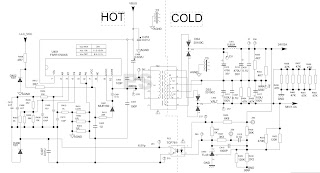
- Power supply Schematic
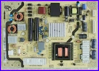
TCL 40-E371C4-PWA1XG
TROUBLESHOOTING
1. Fuse blowing
Check Diode D1 > D4 for any short
Check the IGBT K12A50D For any short.
Replace FAN7930 Pwm driver
2. Power supply doesn’t starts
Check the resistors R307,R308,R309,R310 , is any of them is open or not . This resistor network provides the staring supply to FAN7930.
Replace FAN7930 , FSFR1700XS
Check the diode at the secondary side or the SMPS for any short.
FSFR1700XS
The FSFR-XS series includes highly integrated power switches designed for high-efficiency half-bridge resonant converters. Offering everything necessary to build a reliable and robust resonant converter, the FSFR- XS series simplifies designs while improving productivity and performance. The FSFR-XS series combines power MOSFETs with fast-recovery type body diodes, a high- side gate-drive circuit, an accurate current controlled oscillator, frequency limit circuit, soft-start, and built-in protection functions. The high-side gate-drive circuit has common-mode noise cancellation capability, which guarantees stable operation with excellent noise immunity. The fast-recovery body diode of the MOSFETs improves reliability against abnormal operation conditions, while minimizing the effect of reverse recovery. Using the zero-voltage-switching (ZVS) technique dramatically reduces the switching losses and significantly improves efficiency. The ZVS also reduces the switching noise noticeably, which allows a small- sized Electromagnetic Interference (EMI) filter. The FSFR-XS series can be applied to resonant converter topologies such as series resonant, parallel resonant, and LLC resonant converters.
PIN CONFIGURATION OF FSFR1700XS
1 VDL - This is the drain of the high-side MOSFET, typically connected to the input DC link voltage
2 AR - This pin is for discharging the external soft-start capacitor when any protections are triggered. When the voltage of this pin drops to 0.2 V, all protections are reset and the controller starts to operate again.
3 RT- This pin programs the switching frequency. Typically, an opto-coupler is connected to cont the switching frequency for the output voltage regulation.
4 CS - This pin senses the current flowing through the low-side MOSFET. Typically, negative voltage is applied on this pin.
5 SG - This pin is the control ground.
6 PG - This pin is the power ground. This pin is connected to the source of the low-side MOSFET.
7 LVCC - This pin is the supply voltage of the control IC.
8 NC - No connection.
9 HVCC - This is the supply voltage of the high-side gate-drive circuit IC.
10 VCTR - This is the drain of the low-side MOSFET. Typically, a transformer is connected to this pin.
FAN7930
The FAN7930 is an active power factor correction (PFC)
controller for boost PFC applications that operate in critical conduction mode
(CRM). It uses a voltage-mode PWM that compares an internal ramp signal with
the error amplifier output to generate a MOSFET turn-off signal. Because the
voltage-mode CRM PFC controller does not need rectified AC line voltage
information, it saves the power loss of an input voltage sensing network
necessary for a current-mode CRM PFC controller. FAN793O provides over-voltage
protection, open- feedback protection, over-current protection, input-
voltage-absent detection, and under-voltage lockout protection. The PFC-ready
pin can be used to trigger other power stages when PFC output voltage reaches
the proper level with hysteresis. The FAN7930 can be disabled if the INV pin
voltage is lower than O.45\/ and the operating current decreases to a very low
level. Using a new variable on-time control method, THD is lower than the
conventional CRM boost PFC ICs.
PIN
CONFIGURATION OF
1
INV
This pin is the inverting input of the error amplifier.
The output voltage of the boost PFC converter should be resistively divided to
2.5V.
2
RDY
This pin is used to detect PFC output voltage reaching a
pre-determined value. When output voltage reaches 89% of rated output voltage,
this pin is pulled HIGH, which is an (open drain) output type.
3
COMP
This pin is the output of the transconductance error
amplifier. Components for the output voltage compensation should be connected
between this pin and GND.
4 CS
This pin is the input of the over-current protection
comparator. The MOSFET current is sensed using a sensing resistor and the
resulting voltage is applied to this pin. An internal RC filter is included to
filter switching noise.
5
ZCD
This pin is the input of the zero-current detection
block. If the voltage of this pin goes higher than 1.5V, then goes lower than
1.4V, the MOSFET is turned on.
6
GND
This pin is used for the ground potential of all the
pins. For proper operation, the signal ground and the power ground should be
separated.
7
OUT
This pin is the gate drive output. The peak sourcing and
sinking current levels are +500mA and - 800mA, respectively. For proper
operation, the stray inductance in the gate driving path must be minimized.
8
Vcc
This is the IC supply pin. IC current and MOSFET drive
current are supplied using this pin.
POWER SUPPLY SCHEMATIC DIAGRAM
PFC SECTION
SMPS SECTION
CLICK ON THE IMAGES TO ZOOM IN


